Battery and Energy Technologies |
|
Semiconductors Without the Quantum Physics
(Or not so much that you would notice)
Semiconductor MaterialsOver 600 semiconducting materials are known. They may be elements or compounds and they have a resistivity somewhere between insulators and conductors. Good conductors have resistivity between 10-7Ωm to 10-8 Ωm at room temperature while the resistivity of insulators is in the range1010 Ωm and 1014 Ωm. Semiconductors fall in between with resistivities between 10-6Ωm to 107Ωm, a range of 14 orders of magnitude. Pure semiconductors behave like insulators at 0°Kelvin, however at normal temperatures, in contrast to metals, semiconductors have a negative coefficient of resistance due to the increase in the concentration of charge carriers as the temperature rises as explained below. The properties which make semiconductors interesting are
Energy Bands
Atomic Orbitals The Bohr model of the atom tells us that electrons can only have certain discrete amounts of energy corresponding to certain electron orbits around the atomic nucleus. The notion of distinct planetary electron orbits around an atomic nucleus is a useful shorthand way of explaining some atomic behaviour. Unfortunately it is incorrect. Electrons do not follow defined paths or orbits around the nucleus. The Heisenberg Uncertainty Principle tells us that "it is impossible to define simultaneously, absolute precision, both the position and the momentum of an electron". In other words you can't know with certainty both where an electron is and where it's going to be next. Electrons close to the nucleus can be found anywhere within concentric spherical regions of space, also known confusingly as orbitals or sometimes shells, surrounding, and centred on, the atom's nucleus. The spherical orbitals closer to the nucleus are known as s orbitals. Those at the second energy level and higher, the p, d and f orbitals, may be separated into two or more lobes like balloons tied to the nucleus, the further away from the nucleus, the higher the energy level. σ (sigma) bonds are the strongest type of covalent chemical bond. They are formed by the direct head-on overlapping between atomic orbitals holding a molecule or a crystal together. π (pi) orbitals are weak covalent bonds where just two balloon-like lobes of one involved atomic orbital overlap the two lobes of the other involved atomic orbital. See a diagram of σ and π bonds.
See more about Covalent, Non-covalent and π-π Bonding. Electrons have a minimum energy state and only certain discrete higher energy states are allowed depending on which orbital they inhabit. A fixed amount of energy is needed to pump the electron up into a higher energy state or orbital and when the electron falls back into a lower energy state that energy is given up as electromagnetic radiation. The highest occuped band is called the valence band or sometimes the valence shell. It is the outermost shell of an atom in its uncombined or ground state, and contains the highest energy electrons, that is those most likely to account for the nature of any reactions involving the atom and of the bonding interactions it has with other atoms. The next higher band is the conduction band which is normally empty and may be defined as the lowest unfilled energy band. It is separated from the valence band by an energy gap, also called a band gap. This band gap represents the energy required to knock electrons out of the atom's valence band into the conduction band. Electrons in the conduction band are not tied to the atom from which they originated and can move freely between other atoms. In any material, for conduction to occur, there must be electrons available in the highest energy band. See more about Valency A semiconductor behaves either as a conductor or an insulator depending on whether or not there are free electrons in the conduction band. Once an electron enters the conduction band, it is unbound by the nucleus and free to move within the semiconductor material's crystal structure under the influence of an electric field. The energy required for an electron to jump the band gap can be provided by heat or some form of radiation or from an electric field and is usually expressed in electron Volts (eV) where 1 eV is equivalent to 1.6 X 10⁻¹⁹ Joules (J). In a metal the minimum energy needed to liberate an electron from the surface of the metal is called the "work function". The work function is a constant unique to each element. (Note that the band gap is the difference between two energy levels, not a physical space.)
Molecular Orbitals Fukui showed that the electrons associated with organic molecules, just like those in atoms, are also arranged in energy bands or so called "orbitals" in cloud like shapes ranging from simple spheres, through lozenge shapes to complex multiple lobed shapes depending on the number and nature of the atoms making up the molecule and the module's complexity.. Like atoms, the molecule's energy levels are defined by the arrangement and nature of its orbitals. These are the "highest occupied molecular orbital" or HOMO and the "lowest unoccupied molecular orbital" or LUMO. The HOMO is analogous to the valence band in semiconductors while the LUMO is analogous to the conduction band and the size of the energy band gap between the HOMO and the LUMO enables some organic molecules to act as semiconductors.
Good conductors already have free electrons in the conduction band which are available to carry the current and a small band gap which makes it easy to pump more electrons into the conduction band. Metals have a positive coefficient of resistance since the thermal agitation of the electrons increases with temperature and impedes electron flow. Insulators on the other hand have a wide band gap typically higher than 5 eV (electron Volts) with no electrons in the conduction band. Conduction can occur if a high enough field is used to force electrons into the conduction band but this usually results in the breakdown of the insulating material. Pure semiconductors have few electrons in the conduction band making them poor conductors but their relatively low band gap (0.67 eV for Germanium and 1.12 eV for Silicon) permits their conductivity to be increased by using an external stimulus to raise the energy level of the electrons. When this occurs the higher energy electron it breaks free from the covalent bond between the semiconductor atoms creating an electron-hole pair of new charge carriers thus increasing the conductivity of the semiconductor material. Adding small numbers of new current carriers by doping allows dramatic changes to the conductivity of the semiconductor. Example Semiconductor MaterialsThe unique physical properties of certain materials we now recognise as semiconductors have been known for over a hundred years but it was only in the 1940's that materials were classified as such and their properties were explained. Some examples of semiconductors frequently used in electronics are given below.
Semiconductor DevicesOver 200 device structures have been identified and the principles of operation can be illustrated from some basic types shown here. The list is not exhaustive and many variations on these themes are possible. Note: It must be emphasised that the following explanations are merely a shorthand way of representing the major semiconductor behaviours, sufficient to understand the device functions and the tradeoffs and performance limitations involved in semiconductor device designs. Some minor effects have been omitted. Furthermore, the actual mechanisms involved in the functioning of semiconductor devices are much more complex and are based on quantum physics taking into account the energy levels of the charge carriers and their concentrations and distributions within the semiconductor crystal lattice. Electrons and HolesSemiconductor materials such as Germanium or Silicon are characterized by a valence shell containing four electrons. Each atom has four electrons in its outer orbit and shares these electrons with its four neighbours. Each shared electron pair constitutes a covalent bond. The force of attraction for the electrons by both nuclei holds the two atoms together forming tight crystal structures with no free electrons available to conduct a current. Pure Silicon crystals are therefore insulators. These materials can however be doped to create an excess or lack of electrons, turning the semiconductor into a conductor. Pure semiconductor material without doping is called an intrinsic semiconductor. Heavy doping provides low resistivity materials. Light doping is used for controlled high resistivity. See diagram below. N type materials If small quantities of a different element such as Phosphorus or Arsenic which have five valence electrons in its outer ring are introduced into the crystal lattice of a semiconductor such as Silicon, four of the five electrons will bind with the Silicon atoms leaving one electron unbound and free to move. Semiconductors doped in this way have a surplus of free electrons, or negative charge carriers, available to carry current and are consequently called N type materials. In N type materials the electrons are said to the majority carriers and holes the minority carriers. P type materials In a similar way semiconductors can be doped with elements such as Boron or Indium with only three valence electrons in its outer ring. In this case there will be a shortage of electrons to bind with the Silicon lattice leaving unfilled spaces known as "holes". Electrons can propagate through the crystal like a bubble by filling the neighbouring vacant hole leaving behind a hole in the location it just left. This is equivalent to the propagation of a hole in the opposite direction. Since a hole is essentially the lack of an electron in a neutral material, it must have a net positive charge. Materials with such positive charge carriers are called P type materials. In P type materials the holes are said to be the majority carriers and electrons the minority carriers.
P-N JunctionIn the example above, the Phosphorus atoms create a surplus of electrons in the N type material and the Boron atoms create a surplus of holes or positive carriers in the P type material. Each of these materials standing alone is electrically neutral. However, when a single crystal is doped in the form of a junction, with N type material on one side and P type material on the other side the electrons are attracted by the holes on the other side of the junction and migrate across to bond with them. This leaves the N type material with a net positive charge and the P type material with a net negative charge. The result is that a permanent inherent or "sweeper" electric field is created across the junction. (This region where electrons have diffused across the junction is called the "depletion region" because it no longer contains any mobile charge carriers. It is also known as the "space charge region".) Almost all semiconductor devices depend in some way on the operation of the P-N junction. The simplest of these devices is the diode and we can use the diode to illustrate what happens at the P-N junction. Diode
There will however always be a small, troublesome, temperature dependent leakage current across the junction due to the liberation of new charge carriers caused by thermal effects on the semiconductor material whichever way the diode is biased.
LED's, solar cells, lasers and tunnel diodes are among the many versions of the P-N junction. Varactor DiodeA varactor diode is a variable reactance device. Increasing the reverse bias voltage on a P-N junction forces the charges on either side of the depletion or space charge layer further apart effectively increasing its capacitance. Conversely reducing the bias reduces the capacitance. This property makes the varactor diode ideal for use as a variable capacitor in tuned circuits. Being reverse biased no current flows.
Schottky DiodeSchottky diodes use a metal-semiconductor junction instead of a P-N junction as in conventional diodes. It is electrically similar to a P-N junction, but the current flow in the diode is due primarily to "majority carriers" which means that if the semiconductor body is doped N-type, then the current is carried by only the N-type carriers (mobile electrons ). No slow, random recombination of electrons and holes is involved. This results in both very fast switching times and low forward voltage drop. This same effect however results in poor reverse-bias voltage performance and high reverse leakage currents. Schottky metal-semiconductor contacts can also be used to provide non rectifying, ohmic contacts with a negligible resistance, regardless of the polarity of the applied voltage, to make connections to other devices in an electronic system.
PIN Diode
Avalanche DiodeThe avalanche effect is caused by the breakdown of the P-N junction due to a high reverse voltage field across the depletion layer. As the reverse voltage is increased the very high field across the depletion layer accelerates any charge carriers randomly generated by heat in the layer. In doing so the charge carriers pick up enough energy to raise the energy levels of more electrons when they collide with the crystal lattice giving rise to even more electron-hole pairs creating a self sustaining avalanche effect and a low impedance across the diode. Removing the voltage turns off the current. Zener Diode
Tunnel DiodeLike avalanche and Zener diodes, tunnel diodes are heavily doped and have an extremely narrow depletion or space charge layer of less than 5 to 10 nanometers thick - only a few atoms deep. Similarly they are in breakdown when reverse biased however unlike the other two devices they remain in breakdown for a small initial region of forward biasing, with the breakdown current superimposed on the normal diode forward current.
As the forward voltage increases the diode slowly comes out of breakdown and the total current consequently decreases until breakdown stops and only the normal diode forward current flows, whereupon the current starts to increase again. Normally we would not expect breakdown current to flow in the positive region because the electric field is insufficient to overcome the energy gap necessary to release electrons into the conduction band however the phenomenon is explained by the electrons acting as waves rather than as particles. See Hund (1927) which shows how a certain number of electrons will have more than enough energy to jump an energy gap that would normally be too wide, effectively tunneling through a barrier which we would normally expect bar them. The possibility of unusual applications and very high switching speeds led to great expectations for the tunnel diode but difficulties in manufacturing and advances in other semiconductor technologies have now made it almost obsolete.
Gunn Diode - Transferred Electron Device (TED)An Gunn diode has a voltage current characteristic similar to the tunnel diode (above) but depends on a completely different principle. It has no P-N junction but consists only of N type semiconductor material with different doping concentrations in three distinct regions. The two outer regions connected to the terminals are heavily N doped and a thin layer of lightly doped material is sandwiched in between. When a voltage is applied to the device, the electrical gradient will be largest across the thin middle layer because it is less heavily doped and thus has the highest resistance. Eventually, this layer will start to conduct due to the charge carriers created by the high electric field. The presence of the charge carriers however reduces its resistance and hence the gradient across it, thus preventing further conduction. In practice, this means a Gunn diode has a region of negative differential resistance. Once the current pulse has passed through the middle layer, its resistance of the layer and hence the voltage gradient across it rises again allowing conduction to occur once more. The negative resistance, combined with the transit time across the intermediate layer, allows construction of an RF relaxation oscillator simply by applying a suitable direct current across the device. The oscillation frequency is determined partly by the physical properties of the thin middle layer, but can be controlled by coupling the device with a resonant circuit or cavity. Gunn diodes can used to build oscillators with frequencies up to the teraHertz range.
IMPATT DiodeIMPact Avalanche Transit Time (IMPATT) diodes are two-terminal semiconductor devices that generate RF power by introducing a 180° phase shift between current and voltage waveforms at microwave frequencies. Based on variations of a basic P-N or P-I-N junction, its functions are provided by two operating regions, the avalanche region or injection region which creates the carriers which may be either holes of electrons, and the drift region where the carriers move across the diode taking a certain amount of time dependent upon its thickness and the voltage. The IMPATT diode is thus operated under reverse bias conditions set close to the threshold of avalanche breakdown . An AC voltage superimposed on the DC bias will drive the device into avalanche breakdown during the first half of each AC cycle. The generation of charge carriers by impact ionisation during the first half cycle lags behind the application of the input voltage because carrier generation is not only a function of the electric field but also the number of carriers present. The number of carriers increases as the electric field increases and continues to grow after the field has reached its peak due to the impacts from number of carriers already in existence. This continues until the field falls to below a critical value when the number of carriers starts to fall. As a result of these effects the current generated lags by about 90 degrees behind the voltage. This is known as the injection phase delay.The carrier drift through the depletion region during the second half cycle subjects the carriers to a further delay, producing a displacement current pulse in the external circuit that is 180° out of phase with the voltage. When current and voltage are 180° out of phase, the device is delivering maximum AC power to the external circuit and since the positive voltage produces a negative current, the device can be considered a negative resistance. This temporary negative resistance effect is sufficient take the diode momentarily out of breakdown and is used to generate and sustain an oscillation. IMPATT diodes can produce very high power at microwave frequencies but because they depend on the avalanche process they are hampered by the high level of phase noise they generate.
Light Emitting Diode (LED)LED's depend for their effect on the recombination of electron-hole pairs and the reforming of the covalent bonds in a forward biased diode. When an electron falls back to its unexcited energy level it loses its excess energy which is emitted as a photon of light. The energy in the photon and hence the colour of the light depends on the band gap of the semiconductor. Different materials with different band gaps are needed to produce different colours. This light energy is transmitted out from the device through the sides of the junction region. The light intensity depends on the rate of recombination of the charge carriers and thus the forward current. Not all semiconductors are suitable for making LED's - the conduction band must be directly above the valence band for photon emission. For this reason Gallium Arsenide is a suitable candidate but not Silicon.
Organic Light Emitting Diode (OLED)
|
|||||||||||||||||||||||||||||||||||||||||||||||||||||||||||||||||||||


|
|
When heat is applied to one side of a semiconductor thermocouple the heat energy causes charge carriers to be released into the conduction band, electrons in the N type material and holes in the P type material. The charge carriers concentrated at the hot side of the device will repel eachother with the result is that they tend to migrate towards the cold side of the device. In the N type material this electron flow constitutes a current flowing from the cold side to the hot side and the movement of the electrons causes a negative charge to build up at the cold side with a corresponding positive charge on the hot side due to the deficit of electrons there. In the P type material the migration of the holes constitutes a current flowing in the opposite direction and a positive charge to be built up at the cold side and a corresponding negative charge at the hot side. By connecting the junctions together with metallic interconnections as shown in the diagram above, a current will flow in an external circuit. The current generated is proportional to the temperature gradient between the hot and cold junctions and the voltage is proportional to the temperature difference. Heat must be removed from the cold junction otherwise the migration of the charge carriers will equalise their distribution in the semiconductor eliminating the temperature difference across the device causing the migration and hence the current to stop.
The generation of electrical power from the heat flux passing through a conductor is known as the Seebeck effect.
Thermo-electric generators based on the Seebeck effect have been used in nuclear batteries to harness the heat of nuclear decay to produce electricity.
|
When a voltage is applied across a semiconductor thermocouple, any surplus charge carriers present in the semiconductor will be attracted towards the terminal with the opposite polarity. This is the mechanism of current flow through a conductor. Thus electrons in the N type material migrate towards the positive terminal causing a surplus to accumulate in the region of the semiconductor next to the terminal leaving a deficit at the negative side of the device. Similarly holes in the P type material migrate towards the negative terminal. In other words the charge carriers are swept through the material accelerating as they do so, due to the electric field created by the voltage between the terminals of the device and their increased kinetic energy is manifest as heat. The temperature within the device depends on the number and the kinetic energy of the charge carriers. The temperature will therefore be higher in the region where the charge carriers are concentrated and lower in the region they have just vacated where charge density is consequently lower. Thus a temperature gradient, proportional to the magnitude of the applied current, builds up across the device. This temperature gradient can only be maintained however if heat can be removed from the hot junction, otherwise the temperature will tend to equalise across the device and continued current flow will cause the device to overheat. The heat absorbed or created at the junctions is proportional to the electrical current flow and the proportionality constant is known as the Peltier coefficient. Contrary to Joule heating (I2R), the Peltier effect is reversible depending on the direction of the current.
The heat transfer from one end of a conductor to the other caused by the passage of an electrical current through the conductor is known as the Peltier effect.
|


Semiconducting materials have been used in the example above to illustrate the operating principles of thermoelectricity. The same principles however apply to any conductors. Only the magnitudes of the effects are different.
Though the phenomena of the Seebeck and Peltier effects were first discovered in circuit loops using two dissimilar metals, the fundamental phenomenon actually exists in a single conductor as was later pointed out by Kelvin and named the Thomson effect in his honour. It is thus not the dissimilar metals which generate the voltage but the temperature gradient, it just happened that it was the use of dissimilar metals with different thermal properties in the circuits which enabled the discovery of the phenomena.
Transistors
|
Bipolar Junction Transistors (BJTs) are formed from a three-layer semiconductor sandwich with a very thin middle layer creating two P-N junctions configured like two diodes back to back as in the diagram on the right. In operation one of the junctions is reverse biased the other forward biased. Bipolar Junction Transistors are so named because the main conduction channel employs both electrons and holes to carry the main electric current through the device. The transistor can act as an amplifier or a switch. |
 |
NPN Transistor
In an NPN transistor the outer layers which form the emitter and collector are N type semiconductors doped with an impurity to supply extra electrons, while the thin base layer, typically only 1 micron thick, is a P type semiconductor doped with a different impurity which provides holes.
 A typical NPN transistor is supplied by a positive battery voltage on the collector while the emitter is held at ground potential.
With no voltage, or a negative voltage, on the base, no current, other than leakage current, can flow between the emitter and the collector because the base-collector junction is reverse biased.
If a positive voltage is applied to the base, the emitter-base junction becomes forward biased and electrons flow from the emitter into the base but because the base is very thin and lightly doped only a few electrons recombine with holes and since the reverse biased base-collector junction is depleted of charge carriers, most of the electrons entering the base are swept away towards the positive terminal of the collector flowing across the reverse biased junction.
It is important to keep the base region as thin and as free from defects as possible, in order to minimise recombination losses of the minority carriers (electrons in this case). The current associated with the electron travel, flows in the opposite direction between the collector and the emitter. In this way a small current I(in) entering the base can cause a much larger current I(out) flowing between the collector and the emitter. In other words the transistor acts as an amplifier.
PNP Transistor
 |
In a PNP transistor the emitter and collector are made from P type semiconductors and the base is an N type material. It behaves in a similar way to the NPN transistor except that all the potentials are reversed and the electrons travel in the opposite direction. |
The bipolar junction transistor (BJT) is theoretically a symmetrical device and should operate the same if the emitter and collector leads were interchanged, however in practice the collector is made much larger than the emitter in order to catch as many as possible of the charge carriers provided by the emitter and also to act as a heat sink.
The BJT has traditionally been the analogue designer's transistor of choice, due largely to its high transconductance (the ratio between the change on output current to the voltage change which caused it : gm=ΔIout/ΔVin).
The junction transistor is a current controlled device as opposed to a voltage controlled device and because the base-emitter diode is forward biased, the junction transistor has the disadvantage of a low input impedance which loads down the signal source connected to the transistor base. The FET by contrast is a voltage controlled device and does not have this loading problem since the input diode junction is reversed biased providing a very high input impedance and drawing only very small currents.
The Transistor as a Switch
 |
The transistor is also a fundamental building block of digital circuits. When there is no voltage (a logical "zero") on the base of the transistor the transistor is switched off. Only leakage current, (essentially no current), flows between the collector and the emitter and the transistor acts as an open circuit. Since there is no current through the load resistor, the voltage on the collector will be high, the same as the supply voltage. In digital circuits the high voltage on this output point represents a logical "one" When a positive voltage (a logical "one") is applied to the base, the transistor is switched on. The impedance between the collector and the emitter drops to a low level and current flows through the transistor and the load resistor. Because of the volt drop across the load resistor and the low impedance across the transistor, the voltage on the collector drops to a low level. This means that the output voltage now represents a logical "zero".
See an application in a logic circuit. |
Field Effect Transistors
Bipolar junction transistors are normally-off devices: with no base current, they block any current from going through to the collector. Field-effect transistors are normally-on devices: with zero applied gate-to-source voltage, they allow maximum drain current. They are unipolar devices with the current being carried entirely by majority carriers only and the controlled current does not have to cross a P-N junction. There is a P-N junction inside the FET, but its only purpose is to provide that non conducting depletion region which is used to restrict current through the channel.
In a MOSFET the gate current is negligible and the carriers in the channel are the only types responsible for the current flow.

Junction FET (JFET)
An N channel junction FET is made from a single piece of N type material constricted in the middle by P type material forming the gate. Between the source and the drain, the n-type material acts as a resistor. The current flow consists of the majority carriers (electrons for n-type material).
Since the gate junction is reverse biased and because there is no minority carrier contribution to the flow through the device, the input impedance is extremely high. When the gate voltage is made more negative, it depletes the majority carriers from the constricted current path in the region of the gate increasing its resistance and reducing the current flow. Varying the gate voltage modulates the current flow through the device. The control element for the JFET comes from depletion of charge carriers from the N channel.
Metal Oxide Semiconductor FET (MOSFET) - IGFET
MOSFET's are insulated gate transistors (IGFET's) in which the gate terminal is a metallic layer layer placed over the channel, but separated from it by a thin layer of insulating silicon dioxide. This insulating barrier acts like the dielectric layer of a capacitor, and allows the reverse biased gate-to-source voltage to influence the depletion region electrostatically rather than by direct connection. As in the JFET, varying the voltage on the gate modulates the conductivity of the channel enabling the current flow between drain and source to be controlled. The insulating oxide between the gate and channel effectively isolates a MOSFET in one logic stage from previous and subsequent stages.
The P channel FET works in a similar way to the N channel device with the voltages reversed and with holes rather than electrons as majority carriers.

The MOSFET's are used in the vast majority of digital circuits. See also CMOS
MOSFET technology is also widely used for implementing high power switching devices because of its high input impedance, high switching speed and its thermal stability.
Floating Gate Transistor

The floating-gate, avalanche-injection MOSFET (FAMOS) transistor is the basic building block used to construct the memory cells in non-volatile data storage such as flash , EPROM and EEPROM memory.
In addition to the normal access or control gate these MOSFET's have a second "floating" gate sandwiched between the control gate and the semiconductor substrate embedded within the insulating layer and electrically isolated from both the access gate and the substrate.
Because the floating gate is completely surrounded by SiO2, a high quality insulator, it behaves like a capacitor and any charge placed on the floating gate is prevented from leaking off, thereby providing it with excellent long-term charge retention of 10 years or more.
The device is programmed by applying , a high voltage pulse of 12 Volts or more between the drain and the control gate. Since the SiO2 layer is very thin this causes avalanche breakdown of the gate insulating layer allowing electrons to travel through this SiO2 layer to the floating gate, giving the floating gate electrode an electrical charge.
When the floating gate is charged it modifies the threshold voltage of the control gate inhibiting its operation. Thus it can be set to lock the transistor in its off state, distinguishing it from similar transistors which have not been charged (programmed). This property can be used to provide a read only memory (ROM) function. The floating gate can be restored to its uncharged state by exposure to strong ultraviolet light which causes the charge to leak away.
Arrays of floating gate transistors in integrated circuits are used to provide erasable programmable read-only memory (EPROM). In practice a programmed EPROM retains its data for about ten to twenty years and can be read an unlimited number of times.
Organic Thin Film Transistor
The organic thin film transistor (OTFT) is very similar to the insulated gate field effect transistor (IGFET) described above and works in a similar way with the number of charge carriers flowing between the source and the drain being controlled by the gate. It is however constructed entirely from organic polymer materials which makes it flexible. Because it can be manufactured by a printing process, multiple transistors with their corresponding interconnections can be printed onto large flexible polymer sheets. |
 |
Thyristor or Silicon Controlled Rectifier (SCR)
The thyristor is a four layer P-N-P-N device with different levels of doping for each layer. The cathode is the most heavily doped and the gate and anode are less heavily doped. The central N type layer is only slightly doped and is also thicker than the other layers enabling it to support a high blocking voltage.

In operation the thyristor may be considered as an NPN and a PNP transistor connected back to back, forming a positive feedback loop within the device. The output of one transistor is fed to the input of the second and the output of the second transistor is in turn fed back to the input of the first. A small trigger pulse on the gate will turn the thyristor on and once a current starts to flow, it quickly builds up until both transistors are fully turned on or saturated and the only way it can be turned off is by removing the supply voltage.
The device is designed to act as a switch and can carry very high currents.
Gate Turn Off Thyristor (GTO)
The basic thyristor design suffered from the drawback that once turned on, it could not be turned off unless the supply voltage was removed, since the very high current made a triggered shut off very difficult. By modifying the device structure it was possible to use the same control gate to both turn on and turn off the current flow. However the gate current required to turn off the device may be as much as 20% of the anode (load) current.
As with thyristors these devices can handle very high load currents.
Shockley Diode or Four Layer Diode
The Shockley diode is essentially an SCR without a gate. It is normally normally non-conducting when connected to a low anode voltage but latches on when a voltage pulse in excess of the "breakover" or "firing" voltage is applied and will continue to conduct after the pulse is removed until the anode voltage is removed. It was originally intended for use as a replacement for relays in telecommunications switching applications.
Insulated Gate Bipolar Transistor (IGBT)
The IGBT is a four-layer (N-P-N-P) device similar to a thyristor but with a MOS-gated channel connecting the two n-type regions. It combines the low conduction loss of a BJT with the switching speed of a power MOSFET. The IGBT has high input impedance and fast turn–on speed like a MOSFET and exhibits an on–voltage, current density and low conduction losses comparable to a bipolar transistor but with much faster switching. While some thyristors such as GTOs (Gate Turn Off) are capable of being turned off at the gate, substantial reverse gate current is required, whereas turning off an IGBT only requires that the gate capacitance be discharged and provides a more reliable turn-off. Although turn–on speeds are very fast, turn–off of the IGBT is slower than a MOSFET.
The IGBT is currently the component of choice for high power switching circuits and motor controllers.
Integrated Circuits
Integrated circuits are usually classified according to their circuit functions, of which there are many thousands, or by the device technology. Products range from relatively simple devices made up from combinations of the semiconductor structures noted above, to complete circuits using literally millions of components built onto a single chip. Some simple examples follow of further design possibilities, made possible by integrated circuit fabrication process technology:
Interconnections and passive components
Using doping techniques developed for diodes and transistors it is a easy matter to create on the semiconductor substrate, metallic interconnections, resistors and capacitors which can be used to link active components together in larger circuits.
Capacitors are formed from reverse biased PN junctions. Resistors depend on the ohmic properties of the semiconductor bulk which can be determined by controlled doping with impurities however dc-biased transistors are used to implement high value resistors.
Interconnections depend on the use of the planar construction of the device and are made using photolithography to deposit metallised tracks on top of the Silicon dioxide insulation layer.
New devices can be created by using combinations of the basic semiconductor junctions within the same device. Simple examples are the multiple emitter transistor and the CMOS inverter.
Several discrete devices may be connected together in circuits to implement commonly used electronic functions in notional standard cells. Semiconductor manufacturers maintain cell libraries from which they can draw debugged designs for building more complex circuits. |
 |
|---|
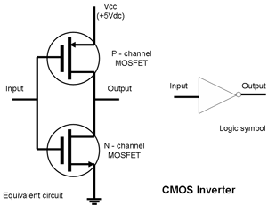 |
Complementary MOSFET (CMOS) CMOS is slightly more complex with P-MOS and N-MOS on the same chip. The configuration shown is an inverting circuit which is the basic component of CMOS logic gates. Only one transistor is "on" at any time but since the other one is "off" no current can flow in the quiescent condition. Current only flows during switching and this combination thus has a very low input power drain, however this also means that the current increases with the clock speed. |
|---|
Mixed technology devices
It is possible to incorporate MOSFET's and BJT's onto the same die to achieve the benefits of both technologies in a single component. In this case low power digital signal processing can be handled by the MOSFET's while the BJT's provide high speed, high current interfacing into the load. BiCMOS (Bipolar-CMOS) and IGBT's (Insulated gate bipolar transistors) are examples of mixed transistor circuits.
Complex circuits
The obvious purpose of integrated circuits is the linking together of discrete components or cells to form complex circuits implemented on a single chip. The microprocessor is probably the most familiar example of this but the possible combinations are endless.
Semiconductor materials performance goals
- High purity semiconducting materials - No unwanted or uncontrolled conducting properties.
- Defect free crystals - Dislocations disrupt device structures.
- Extremely thin transistor base layers - Assists migration of minority carriers across the base, reduces device capacitance and increases upper frequency limit.
- Very small structures - Minimise device real estate.
- Short connections - Reduce electron transit times, increase frequency range, reduce die size.
- Large collector area and mass - Assist high power handling
- High temperature operating capability
- Good thermal conductor - Easy heat removal
- Low leakage currents - Switches that are truly "off" when they are supposed to be off.
- Readily accepts doping
- Easy to work with - No expensive manufacturing techniques
- Inexpensive material
Manufacturing
The methods of designing and building these clever semiconductor structures requires engineers skilled in a wide range of subjects from electronic circuits and software to optics, X-ray crystallography and quantum theory and called for the development of innovative precision manufacturing techniques and process controls.
The following are some of the physical (mechanical) structures which have been used for implementing the electrical structures noted above and the manufacturing processes used to achieve them:
- Point contact transistor (1947)
- Single crystal growth (1948)
- Grown junction transistors (1950)
- Alloy junction transistors (1951)
- Zone refining (1952)
- Diffusion (1952)
- Surface barrier transistor (1953)
- Ion implantation (1954)
- Diffused base transistor (1954)
- Mesa transistor (1954)
- Photolithography (1955)
- Silicon dioxide masking (1957)
- Planar transistor (1958)
- Integrated circuit (1958-59)
- MOSFET (1960)
- Epitaxial deposition (1960)
- Logic families (1961)
- Operational amplifiers (1962)
- Electron beam lithography (1967)
- Application-Specific Integrated Circuits (ASIC's) (1967)
- Memory (1970)
- Microprocessor (1971)
- Projection printing (1973)
- Programmable Logic Device (PLD) (1977)
- Step and repeat (1978)
- Digital Signal Processor (1978)
- Very Large Scale Integrated Circuits (VLSI) (1980)
- Field Programmable Gate Array (FPGA) (1984)
Polish Translation By Natasha Singh
![]() Print This Page || Home || FAQ || Site Map || Legal || Privacy Promise || Contacts
Print This Page || Home || FAQ || Site Map || Legal || Privacy Promise || Contacts
Woodbank Communications Ltd, South Crescent Road, Chester, CH4 7AU, (United Kingdom)
Copyright © Woodbank Communications Ltd 2005
